1
Data sheet acquired from Harris Semiconductor
SCHS164
Features
∑ Four Operating Modes
- Shift Right, Shift Left, Hold and Reset
∑ Synchronous Parallel or Serial Operation
∑ Typical f
MAX
= 60MHz at V
CC
= 5V, C
L
= 15pF,
T
A
= 25
o
C
∑ Asynchronous Master Reset
∑ Fanout (Over Temperature Range)
- Standard Outputs . . . . . . . . . . . . . . . 10 LSTTL Loads
- Bus Driver Outputs . . . . . . . . . . . . . 15 LSTTL Loads
∑ Wide Operating Temperature Range . . . -55
o
C to 125
o
C
∑ Balanced Propagation Delay and Transition Times
∑ Significant Power Reduction Compared to LSTTL
Logic ICs
∑ HC Types
- 2V to 6V Operation
- High Noise Immunity: N
IL
= 30%, N
IH
= 30% of V
CC
at V
CC
= 5V
∑ HCT Types
- 4.5V to 5.5V Operation
- Direct LSTTL Input Logic Compatibility,
V
IL
= 0.8V (Max), V
IH
= 2V (Min)
- CMOS Input Compatibility, I
l
1
µ
A at V
OL
, V
OH
Description
The Harris CD74HC194 and CD74HCT194 are 4-bit shift
registers with Asynchronous Master Reset (MR). In the par-
allel mode (S0 and S1 are high), data is loaded into the
associated flip-flop and appears at the output after the posi-
tive transition of the clock input (CP). During parallel loading
serial data flow is inhibited. Shift left and shift right are
accomplished synchronously on the positive clock edge with
serial data entered at the shift left (DSL) serial input for the
shift right mode, and at the shift right (DSR) serial input for
the shift left mode. Clearing the register is accomplished by
a Low applied to the Master Reset (MR) pin.
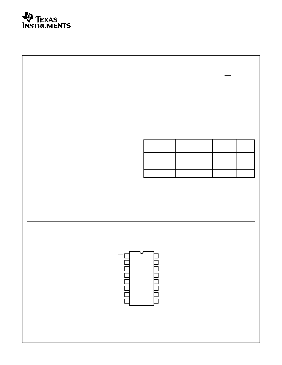
Pinout
CD74HC194, CD74HCT194
(PDIP, SOIC)
TOP VIEW
Ordering Information
PART NUMBER
TEMP. RANGE (
o
C)
PACKAGE
PKG.
NO.
CD74HC194E
-55 to 125
16 Ld PDIP
E16.3
CD74HCT194E
-55 to 125
16 Ld PDIP
E16.3
CD74HC194M
-55 to 125
16 Ld SOIC
M16.15
NOTES:
1. When ordering, use the entire part number. Add the suffix 96 to
obtain the variant in the tape and reel.
2. Die for this part number is available which meets all electrical
specifications. Please contact your local sales office or Harris
customer service for ordering information.
14
15
16
9
13
12
11
10
1
2
3
4
5
7
6
8
MR
DSR
D
0
D
1
D
2
D
3
GND
DSL
V
CC
Q
1
Q
2
Q
3
CP
S1
S0
Q
0
September 1997
CAUTION: These devices are sensitive to electrostatic discharge. Users should follow proper IC Handling Procedures.
Copyright
©
Harris Corporation 1997
CD74HC194,
CD74HCT194
High-Speed CMOS Logic
4-Bit Bidirectional Universal Shift Register
File Number
1668.1
[ /Title
(CD74
HC194,
CD74H
CT194)
/Sub-
ject
(High-
Speed
CMOS
Logic
4-Bit
2
Functional Diagram
14
12
13
15
Q
0
Q
1
Q
2
Q
3
7
6
3
4
5
D
0
D
1
D
2
D
3
GND = 8
V
CC
= 16
2
9
10
1
11
DSL
DSR
S0
S1
MR
CP
TRUTH TABLE
OPERATING
MODE
INPUTS
OUTPUT
CP
MR
S1
S0
DSR
DSL
D
n
Q
0
Q
1
Q
2
Q
3
Reset (Clear)
X
L
X
X
X
X
X
L
L
L
L
Hold (Do Nothing)
X
H
l (Note 2)
l (Note 2)
X
X
X
q
0
q
1
q
2
q
3
Shift Left
H
h
l (Note 2)
X
l
X
q
1
q
2
q
3
L
H
h
l (Note 2)
X
h
X
q
1
q
2
q
3
H
Shift Right
H
l (Note 2)
h
l
X
X
L
q
0
q
1
q
2
H
l (Note 2)
h
h
X
X
H
q
0
q
1
q
2
Parallel Load
H
h
h
X
X
d
n
d
0
d
1
q
2
d
3
NOTES:
1. H = High Voltage Level,
h = High Voltage Level One Set-up Time Prior To The Low to High Clock Transition,
L = Low Voltage Level,
l = Low Voltage Level One Set-up Time Prior to the Low to High Clock Transition,
d
n
(q
n
) = Lower Case Letters Indicate the State of the Referenced Input (or output) One Set-up Time Prior to the Low To High Clock
Transition,
X = Don't Care,
= Transition from Low to High Level
2. The High to Low transition of the S0 and S1 Inputs on the CD74HC194, CD74HCT194 should only take place while CP is High for
Conventional Operation.
CD74HC194, CD74HCT194
3
Absolute Maximum Ratings
Thermal Information
DC Supply Voltage, V
CC
. . . . . . . . . . . . . . . . . . . . . . . . -0.5V to 7V
DC Input Diode Current, I
IK
For V
I
< -0.5V or V
I
> V
CC
+ 0.5V
. . . . . . . . . . . . . . . . . . . . . .±
20mA
DC Output Diode Current, I
OK
For V
O
< -0.5V or V
O
> V
CC
+ 0.5V
. . . . . . . . . . . . . . . . . . . .±
20mA
DC Output Source or Sink Current per Output Pin, I
O
For V
O
> -0.5V or V
O
< V
CC
+ 0.5V
. . . . . . . . . . . . . . . . . . . .±
25mA
DC V
CC
or Ground Current, I
CC or
I
GND
. . . . . . . . . . . . . . . . . .±
50mA
Operating Conditions
Temperature Range (T
A
) . . . . . . . . . . . . . . . . . . . . . -55
o
C to 125
o
C
Supply Voltage Range, V
CC
HC Types . . . . . . . . . . . . . . . . . . . . . . . . . . . . . . . . . . . . .2V to 6V
HCT Types . . . . . . . . . . . . . . . . . . . . . . . . . . . . . . . . .4.5V to 5.5V
DC Input or Output Voltage, V
I
, V
O
. . . . . . . . . . . . . . . . . 0V to V
CC
Input Rise and Fall Time
2V . . . . . . . . . . . . . . . . . . . . . . . . . . . . . . . . . . . . . . 1000ns (Max)
4.5V. . . . . . . . . . . . . . . . . . . . . . . . . . . . . . . . . . . . . . 500ns (Max)
6V . . . . . . . . . . . . . . . . . . . . . . . . . . . . . . . . . . . . . . . 400ns (Max)
Thermal Resistance (Typical, Note 3)
JA
(
o
C/W)
PDIP Package . . . . . . . . . . . . . . . . . . . . . . . . . . . . .
90
SOIC Package . . . . . . . . . . . . . . . . . . . . . . . . . . . . .
190
Maximum Junction Temperature . . . . . . . . . . . . . . . . . . . . . . . 150
o
C
Maximum Storage Temperature Range . . . . . . . . . .-65
o
C to 150
o
C
Maximum Lead Temperature (Soldering 10s) . . . . . . . . . . . . . 300
o
C
(SOIC - Lead Tips Only)
CAUTION: Stresses above those listed in "Absolute Maximum Ratings" may cause permanent damage to the device. This is a stress only rating and operation
of the device at these or any other conditions above those indicated in the operational sections of this specification is not implied.
NOTE:
3.
JA
is measured with the component mounted on an evaluation PC board in free air.
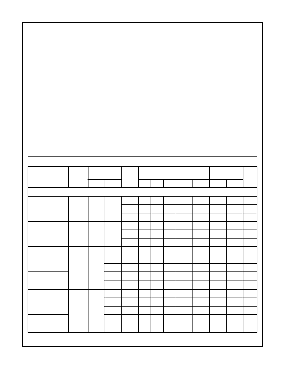
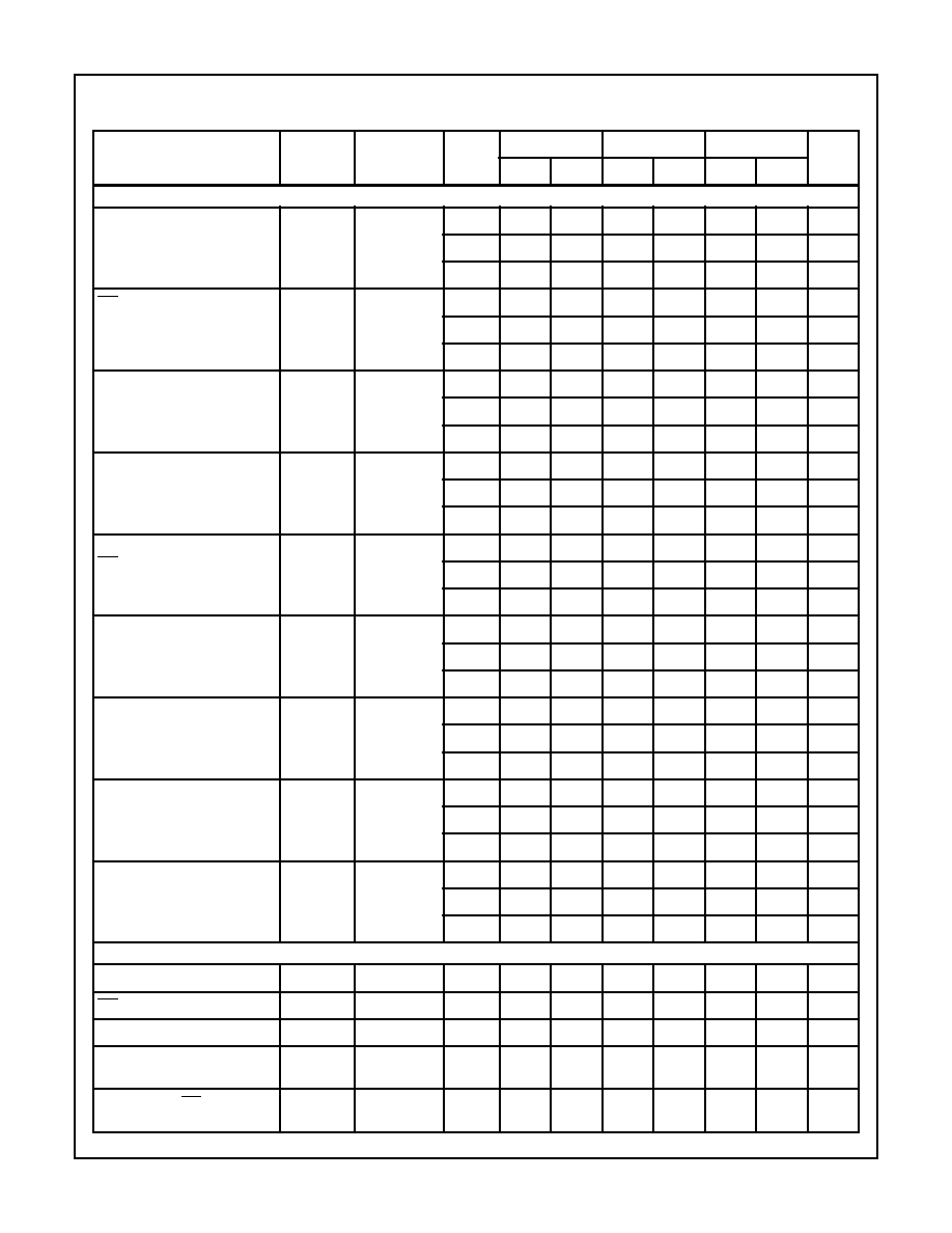
DC Electrical Specifications
PARAMETER
SYMBOL
TEST
CONDITIONS
V
CC
(V)
25
o
C
-40
o
C TO 85
o
C
-55
o
C TO 125
o
C
UNITS
V
I
(V)
I
O
(mA)
MIN
TYP
MAX
MIN
MAX
MIN
MAX
HC TYPES
High Level Input
Voltage
V
IH
-
-
2
1.5
-
-
1.5
-
1.5
-
V
4.5
3.15
-
-
3.15
-
3.15
-
V
6
4.2
-
-
4.2
-
4.2
-
V
Low Level Input
Voltage
V
IL
-
-
2
-
-
0.5
-
0.5
-
0.5
V
4.5
-
-
1.35
-
1.35
-
1.35
V
6
-
-
1.8
-
1.8
-
1.8
V
High Level Output
Voltage
CMOS Loads
V
OH
V
IH
or
V
IL
-0.02
2
1.9
-
-
1.9
-
1.9
-
V
-0.02
4.5
4.4
-
-
4.4
-
4.4
-
V
-0.02
6
5.9
-
-
5.9
-
5.9
-
V
High Level Output
Voltage
TTL Loads
-4
4.5
3.98
-
-
3.84
-
3.7
-
V
-5.2
6
5.48
-
-
5.34
-
5.2
-
V
Low Level Output
Voltage
CMOS Loads
V
OL
V
IH
or
V
IL
0.02
2
-
-
0.1
-
0.1
-
0.1
V
0.02
4.5
-
-
0.1
-
0.1
-
0.1
V
0.02
6
-
-
0.1
-
0.1
-
0.1
V
Low Level Output
Voltage
TTL Loads
4
4.5
-
-
0.26
-
0.33
-
0.4
V
5.2
6
-
-
0.26
-
0.33
-
0.4
V
CD74HC194, CD74HCT194
4
Input Leakage
Current
I
I
V
CC
or
GND
-
6
-
-
±
0.1
-
±
1
-
±
1
µ
A
Quiescent Device
Current
I
CC
V
CC
or
GND
0
6
-
-
8
-
80
-
160
µ
A
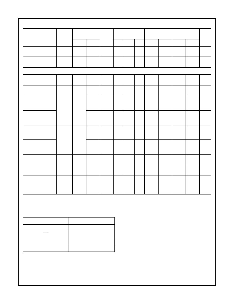
HCT TYPES
High Level Input
Voltage
V
IH
-
-
4.5 to
5.5
2
-
-
2
-
2
-
V
Low Level Input
Voltage
V
IL
-
-
4.5 to
5.5
-
-
0.8
-
0.8
-
0.8
V
High Level Output
Voltage
CMOS Loads
V
OH
V
IH
or
V
IL
-0.02
4.5
4.4
-
-
4.4
-
4.4
-
V
High Level Output
Voltage
TTL Loads
-4
4.5
3.98
-
-
3.84
-
3.7
-
V
Low Level Output
Voltage
CMOS Loads
V
OL
V
IH
or
V
IL
0.02
4.5
-
-
0.1
-
0.1
-
0.1
V
Low Level Output
Voltage
TTL Loads
4
4.5
-
-
0.26
-
0.33
-
0.4
V
Input Leakage
Current
I
I
V
CC
to
GND
0
5.5
-
-
±
0.1
-
±
1
-
±
1
µ
A
Quiescent Device
Current
I
CC
V
CC
or
GND
0
5.5
-
-
8
-
80
-
160
µ
A
Additional Quiescent
Device Current Per
Input Pin: 1 Unit Load
(Note 4)
I
CC
V
CC
-2.1
-
4.5 to
5.5
-
100
360
-
450
-
490
µ
A
NOTE:
4. For dual-supply systems theoretical worst case (V
I
= 2.4V, V
CC
= 5.5V) specification is 1.8mA.
DC Electrical Specifications
(Continued)
PARAMETER
SYMBOL
TEST
CONDITIONS
V
CC
(V)
25
o
C
-40
o
C TO 85
o
C
-55
o
C TO 125
o
C
UNITS
V
I
(V)
I
O
(mA)
MIN
TYP
MAX
MIN
MAX
MIN
MAX
HCT Input Loading Table
INPUT
UNIT LOADS
CP
0.6
MR
0.55
DSL, DSR, D
n
0.25
Sn
1.10
NOTE: Unit Load is
I
CC
limit specified in DC Electrical
Specifications table, e.g. 360
µ
A max at 25
o
C.
CD74HC194, CD74HCT194
5
Prerequisite For Switching Function
PARAMETER
SYMBOL
TEST
CONDITIONS V
CC
(V)
25
o
C
-40
o
C TO 85
o
C
-55
o
C TO 125
o
C
UNITS
MIN
MAX
MIN
MAX
MIN
MAX
HC TYPES
Max. Clock Frequency
(Figure 1)
f
MAX
-
2
6
-
5
-
4
-
MHz
4.5
30
-
24
-
20
-
MHz
6
35
-
28
-
23
-
MHz
MR Pulse Width
(Figure 2)
t
W
-
2
80
-
100
-
120
-
ns
4.5
16
-
20
-
24
-
ns
6
14
-
17
-
20
-
ns
Clock Pulse Width
(Figure 1)
t
W
-
2
80
-
100
-
120
-
ns
4.5
16
-
20
-
24
-
ns
6
14
-
17
-
20
-
ns
Set-up Time
Data to Clock (Figure 3)
t
SU
-
2
70
-
90
-
105
-
ns
4.5
14
-
18
-
21
-
ns
6
12
-
15
-
19
-
ns
Removal Time,
MR to Clock (Figure 2)
t
REM
-
2
60
-
75
-
90
-
ns
4.5
12
-
15
-
18
-
ns
6
10
-
13
-
15
-
ns
Set-Up Time
S1, S0 to Clock (Figure 4)
t
SU
-
2
80
-
100
-
120
-
ns
4.5
16
-
20
-
24
-
ns
6
14
-
17
-
20
-
ns
Set-up Time
DSL, DSR to Clock (Figure 4)
t
SU
-
2
70
-
90
-
105
-
ns
4.5
14
-
18
-
21
-
ns
6
12
-
15
-
18
-
ns
Hold Time
S1, S0 to Clock (Figure 4
t
H
-
2
0
-
0
-
0
-
ns
4.5
0
-
0
-
0
-
ns
6
0
-
0
-
0
-
ns
Hold Time
Data to Clock (Figure 3)
t
H
-
2
0
-
0
-
0
-
ns
4.5
0
-
0
-
0
-
ns
6
0
-
0
-
0
-
ns
HCT TYPES
Max. Clock Frequency (Figure 1)
f
MAX
-
4.5
27
-
22
-
18
-
MHz
MR Pulse Width (Figure 2)
t
W
-
4.5
16
-
20
-
24
-
ns
Clock Pulse Width (Figure 1)
t
W
-
4.5
16
-
20
-
24
-
ns
Set-up Time, Data to Clock
(Figure 3)
t
SU
-
4.5
14
-
18
-
21
-
ns
Removal Time MR to Clock
(Figure 2)
t
REM
-
4.5
12
-
15
-
18
-
ns
CD74HC194, CD74HCT194